Next-Generation Plasma-Resistant Coating Technology—Y Coating
一、Introduction
One of the key factors affecting wafer yield today lies in the durability of components within etching equipment. These parts are continuously exposed to high-energy plasma environments and are highly susceptible to corrosion and erosion. Once the protective coating degrades and begins to peel, particles and dust may be released into the chamber, increasing the risk of wafer contamination and yield loss. As semiconductor line widths continue to shrink, the tolerance for particle defects becomes even lower. Therefore, the development of next-generation plasma-resistant coating technologies is essential to ensuring process stability and long-term reliability in advanced semiconductor manufacturing.
二、Current Industry Practices and Their Limitations
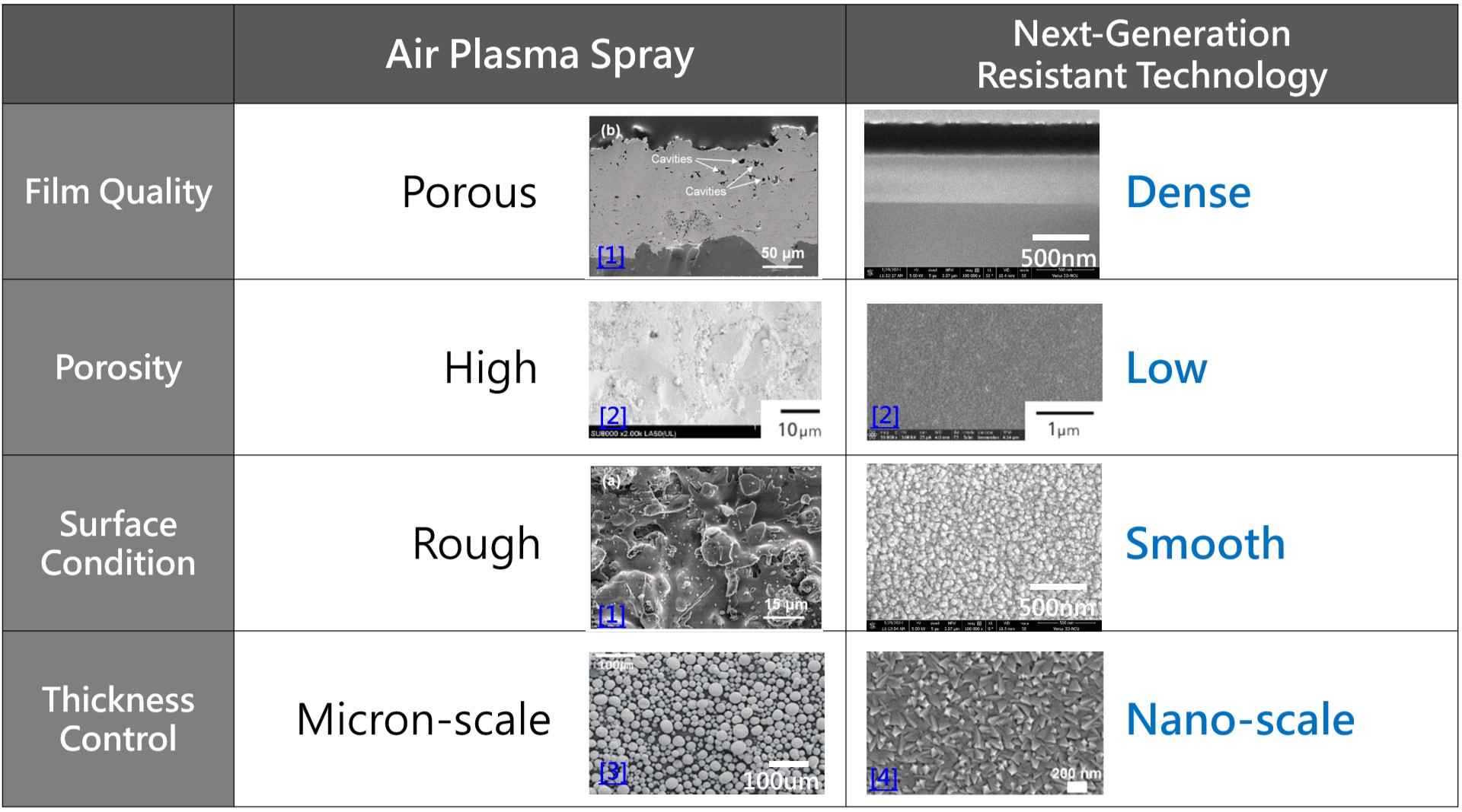
The mainstream industry approach currently adopts Atmospheric Plasma Spraying (APS) technology, using yttrium-based compounds (Y-Coating) to form a protective anti-plasma etch layer on substrate surfaces. APS offers a cost-effective corrosion resistance solution under relatively low-temperature conditions. However, the resulting coatings tend to have porous surface structures, which allow fluorine ions to penetrate and corrode, compromising coating lifespan and process stability. While this technology was widely used five years ago, the continuous shrinkage of line widths has made APS increasingly inadequate in meeting the stringent demands for film density and particle control in today’s advanced processes.
Dah Young Vacuum introduces a next-generation anti-plasma etch coating technology, featuring highly dense, strongly adherent, and ultra-pure coatings—delivering a more stable and long-lasting solution to meet the challenges of advanced semiconductor processing.
三、Next-Generation Plasma Corrosion-Resistant Technology
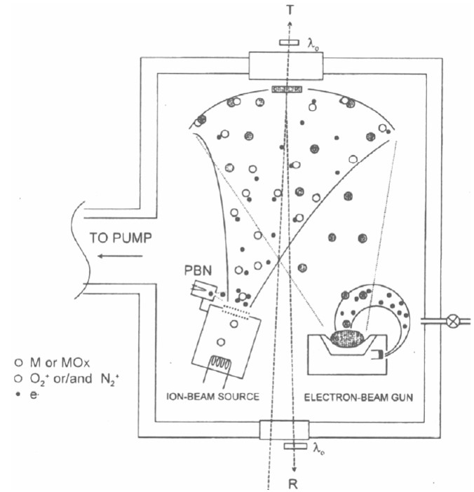
Physical Vapor Deposition (PVD) is a process in which solid materials are vaporized, transported in gas phase, and then condensed as a thin film on the substrate surface. Ion Assisted Electron Beam Evaporation (IAD) builds upon PVD by introducing high-energy ions during deposition. These ions, characterized by their high mass and kinetic energy, bombard the substrate, enabling the formation of films that are denser, purer, and more structurally ordered than conventional coatings.
Compared to traditional Air Plasma Spray (APS), IAD produces coatings with lower porosity, smoother surfaces, and nanometer-level thickness control, making it especially suitable for modern semiconductor components with shrinking line widths. This technology eliminates the limitations of APS, which is generally restricted to large-scale substrates, and offers a next-generation solution for plasma-resistant thin films in advanced microfabrication environments.
四、Conclusion
As Air Plasma Spray (APS) gradually falls short of the demands of modern semiconductor manufacturing, the industry urgently requires a next-generation solution for plasma etch resistance. At Dah Young Vacuum, we firmly believe that Ion Assisted Electron Beam Evaporation (IAD) is the ideal answer.
IAD significantly overcomes the limitations of APS by producing coatings with dense, uniform structures that effectively block fluorine ion infiltration through pores or grain boundaries, thus preventing component corrosion and delamination. Moreover, this advanced process enables nanometer-level thickness control, fully aligned with today’s increasingly miniaturized line widths and spacing requirements.
By choosing our next-generation IAD
coating technology, long-lasting and reliable etch components are no longer out of reach. Improve yield, reduce contamination risks, and secure process stability with a future-ready solution from Dah Young Vacuum.