A Method for Preparing Silicon Carbide Compound
Patent Certificate Number: I860660
Title:A Method for Preparing Silicon Carbide Compound
[1] Patent Claims
- A method for preparing a silicon carbide compound, comprising the steps of: providing a hollow cathode unit comprising two silicon targets placed in parallel inside a mask, forming a slit between the two silicon targets, including a slit inlet and a slit outlet; applying a plasma power to the two silicon targets in a reduced-pressure environment to generate a hollow cathode discharge silicon plasma; introducing a sputtering gas through the slit inlet to blow the hollow cathode discharge silicon plasma out of the slit outlet, and introducing a hydrocarbon gas near the slit outlet; reacting the hollow cathode discharge silicon plasma with the hydrocarbon gas to form a silicon carbide compound thin film that coats at least part or the entire surface of a substrate; and controlling the Si/C molar ratio of the silicon carbide compound thin film by adjusting the flow rates of the sputtering gas and/or the hydrocarbon gas.
- The method according to claim 1, wherein the flow rates of the sputtering gas and/or the hydrocarbon gas are controlled by a mass flow controller.
- The method according to claim 1 or 2, wherein the silicon targets comprise single crystal silicon, polycrystalline silicon, amorphous silicon, or a combination thereof.
- The method according to claim 1 or 2, wherein the sputtering gas includes inert gases.
- The method according to claim 4, wherein the inert gases include helium, argon, and krypton.
- The method according to claim 1 or 2, wherein the hydrocarbon gas includes methane, ethane, ethylene, propylene, or acetylene.
- The method according to claim 1 or 2, wherein the substrate includes metal or non-metal materials.
- The method according to claim 7, wherein the non-metal substrate includes ceramics or polymers.
- The method according to claim 1 or 2, wherein the silicon carbide compound thin film is a compound formed by the reaction of silicon and carbon, with a molecular formula comprising SixCy, where x and y are arbitrary constants and the molar ratio x/y is an arbitrary constant.
- To better illustrate the technical solutions of the embodiments of this invention, the following briefly introduces the drawings used in the description of the embodiments. Obviously, the drawings described below are only some examples or embodiments of this invention and do not limit the technical scope of the invention. Unless otherwise apparent from the context or explained, the same reference numerals in the drawings represent the same structures or operations. Among them:
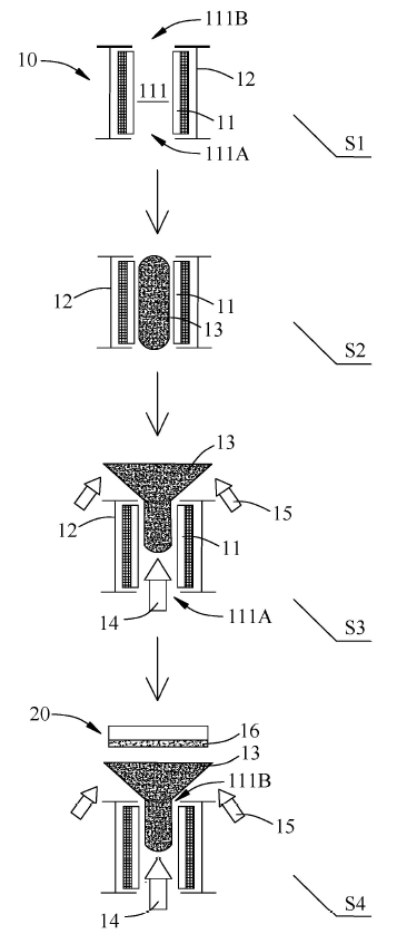
- Figure 1 is a schematic flow diagram of a preferred embodiment of the method for preparing a silicon carbide compound according to this invention.
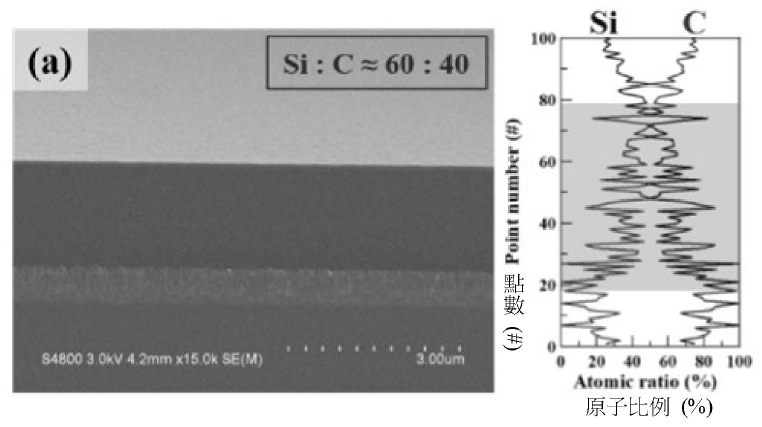
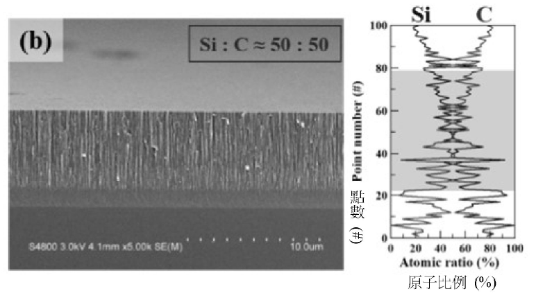
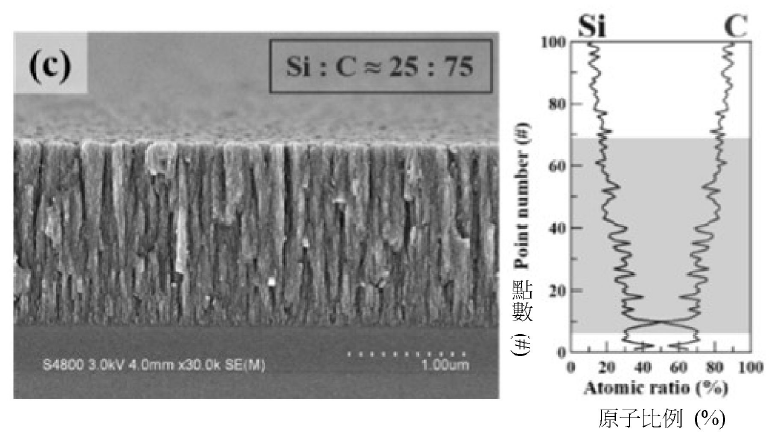
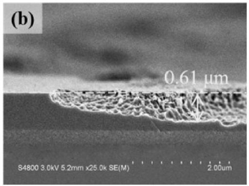
- Figures 2a to 2c show the cross-sectional microstructure and compositional distribution maps of the silicon carbide compound thin films obtained at different acetylene flow rates: (a) 20 sccm, (b) 30 sccm, and (c) 50 sccm in the preferred embodiment.
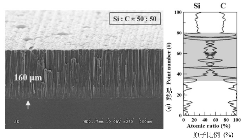
- Figure 3 shows the cross-sectional microstructure and compositional distribution maps of the silicon carbide compound thin film obtained after a 16-hour process time in the preferred embodiment.
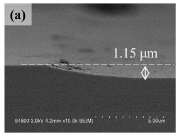
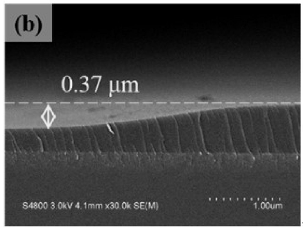
- Figure 4a is the cross-sectional microstructure of a bare silicon wafer control sample after plasma etching for 200 seconds in SiF6 atmosphere.
- Figure 4b is the cross-sectional microstructure after plasma etching for 200 seconds in SiF6 atmosphere of the preferred embodiment.
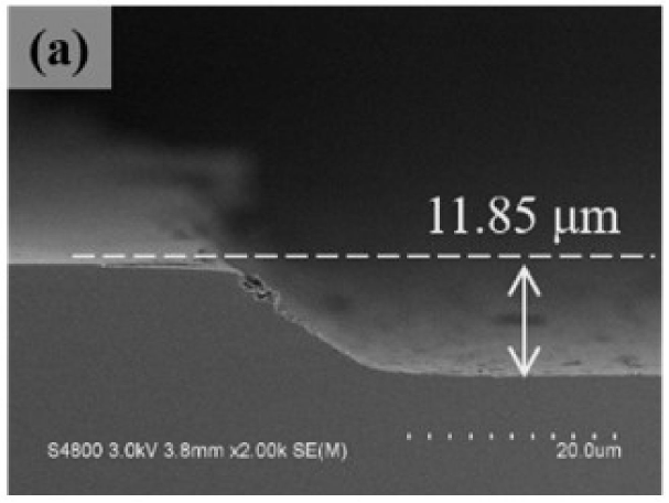
- Figure 5a is the cross-sectional microstructure of a bare silicon wafer control sample after plasma etching for 200 seconds in SiF6 and Cl2 atmospheres.
-
Figure 5b is the cross-sectional microstructure after plasma etching for 200 seconds in SiF6 and Cl2 atmospheres of the preferred embodiment.
[Figure 1]
[Figure 2a]
[Figure 2b]
[Figure 2c]
[Figure 3]
[Figure 4a]
[Figure 4b]
[Figure 5a]
[Figure 5b]