Semiconductor Process Equipment Component and Manufacturing Method Thereof
Patent Certificate Number: I806656
Title:Semiconductor Process Equipment Component and Manufacturing Method Thereof
[1] Patent Claims
- A component suitable for semiconductor process equipment, the component comprising: a substrate made of silicon; and a protective coating covering at least a portion of the substrate; wherein the carbon atom ratio in the protective coating increases in a direction away from the substrate, and the silicon atom ratio in the protective coating decreases in said direction; and wherein, near the substrate, the silicon atom ratio in the protective coating is greater than the carbon atom ratio, and near an outer surface of the protective coating, the silicon atom ratio in the protective coating is less than the carbon atom ratio.
- The component of claim 1, wherein the silicon atom ratio near the substrate is greater than 50%, and the carbon atom ratio near the outer surface of the protective coating is greater than 50%.
- The component of claim 1, wherein the protective coating includes crystalline silicon having (111) crystal plane, (220) crystal plane, or a combination of the aforementioned crystal planes.
- The component of claim 1, wherein the protective coating includes 3C-SiC formed by reactive physical vapor deposition, and the 3C-SiC includes amorphous silicon carbide or crystalline silicon carbide having (111) crystal plane.
- The component of claim 1, wherein a relative content ratio of silicon to carbon in the protective coating is 2/3 to 3/2.
- The component of claim 1, wherein the protective coating has a first portion and a second portion, the first portion is connected to the substrate and the second portion, and the silicon atom ratio near the substrate is greater than the silicon atom ratio of the second portion.
- The component of claim 6, wherein the protective coating further has a third portion, the third portion is connected to the second portion and opposite to the first portion, the carbon atom ratio of the third portion is greater than the carbon atom ratio of the first portion near the substrate.
- The component of claim 1, wherein the protective coating has a crystallinity between 0% and 60%.
- The component of claim 1, wherein when a reactive gas including gaseous SF6 and Cl2 is used in a dry etcher in reactive ion etching (RIE) mode, a relative etching rate of the protective coating relative to the substrate is not greater than 3/5.
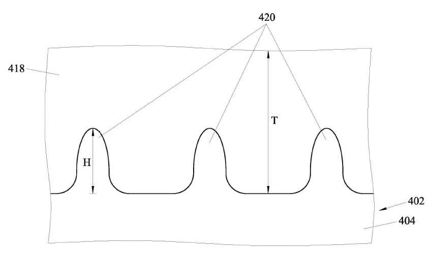
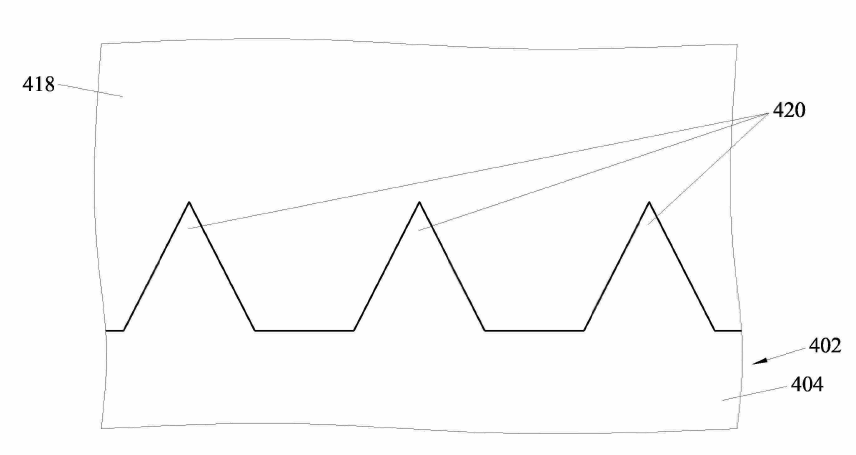
- The component of claim 1, wherein the substrate has a surface including a plurality of microstructures, each microstructure has a height between 300nm and 1.5μm, and the protective coating has a minimum thickness of not less than 10μm.
- The component of claim 1, wherein the protective coating has a minimum thickness of not less than 1.5μm.
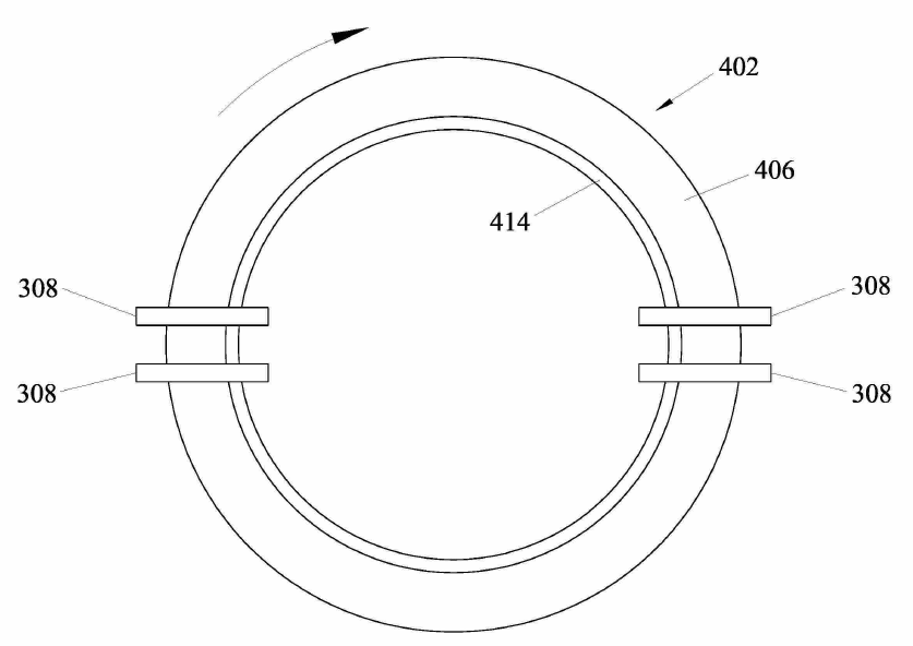
- The component of claim 1, wherein the component is a closed-loop object.
- The component of claim 12, wherein the closed-loop object is a focus ring for use in a dry etching equipment.
- A component suitable for semiconductor process equipment, the component comprising: a substrate; and a protective coating covering at least a portion of the substrate; wherein the protective coating includes 3C-SiC formed by reactive physical vapor deposition, and the 3C-SiC includes amorphous silicon carbide or crystalline silicon carbide having (111) crystal plane, and the protective coating includes crystalline silicon having (111) crystal plane, (220) crystal plane, or a combination of the aforementioned crystal planes.
- The component of claim 14, wherein a relative content ratio of silicon to carbon in the protective coating is 2/3 to 3/2.
- The component of claim 14, wherein the protective coating has a crystallinity between 0% and 60%.
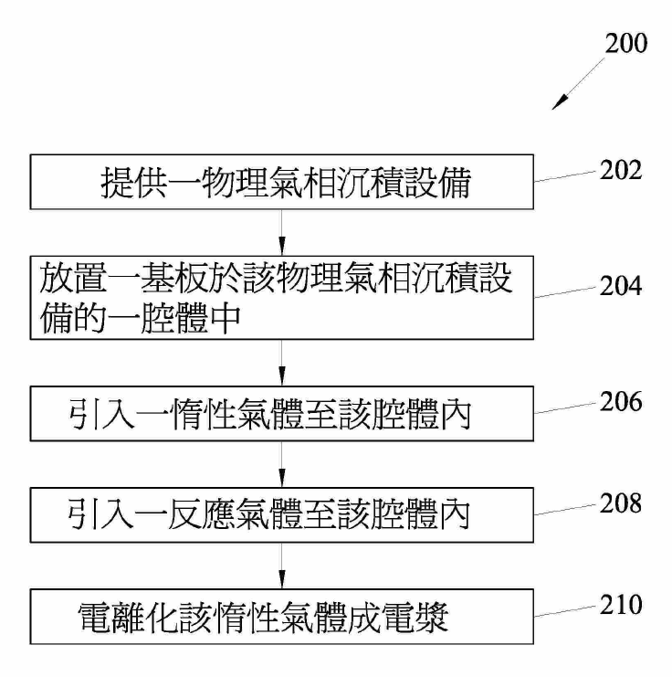
- A manufacturing method for a component suitable for semiconductor process equipment, the method comprising: introducing an inert gas into a chamber containing a plurality of silicon targets and a substrate; introducing a reactive gas containing carbon element into the chamber; and ionizing the inert gas into plasma, causing the plasma to bombard the silicon targets to cause silicon atoms to detach from the silicon targets and react with the reactive gas, thereby forming a silicon carbide protective coating covering at least a portion of the substrate.
- The manufacturing method of claim 17, wherein the substrate is made of silicon, silicon oxide, graphite, ceramic, metal, or alloy.
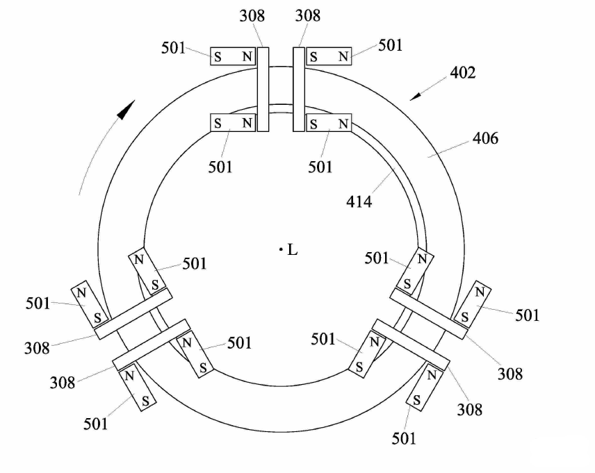
- The manufacturing method of claim 17, further comprising placing an even number of silicon targets in the chamber before introducing the inert gas and the reactive gas, the silicon targets being arranged as at least one pair of silicon targets facing each other.
- The manufacturing method of claim 19, further comprising rotating the substrate as a closed-loop object around a virtual central axis.
- The manufacturing method of claim 17, further comprising: biasing the substrate to cause at least a portion of ions of the plasma to bombard the substrate to remove oxide layers on the substrate and generate dangling bonds on the surface of the substrate; wherein the protective coating is formed on the substrate through chemical bonding with the dangling bonds.
- The manufacturing method of claim 17, further comprising heating or annealing the substrate to a temperature below the melting point of silicon carbide and the substrate.
- The manufacturing method of claim 17, wherein at least one of a flow rate of the inert gas, a flow rate of the reactive gas, and a radio frequency power used to ionize the inert gas dynamically changes and ends with a greater value compared to an initial value during the formation process of the protective coating.
- The manufacturing method of claim 23, wherein the flow rate of the inert gas ranges from 5 slm to 24 slm, the flow rate of the reactive gas ranges from 10 sccm to 120 sccm, and the radio frequency power ranges from 0.4 kW to 1.2 kW.
- The manufacturing method of claim 17, wherein a formation rate of the protective coating is not less than 6Å/sec.
-
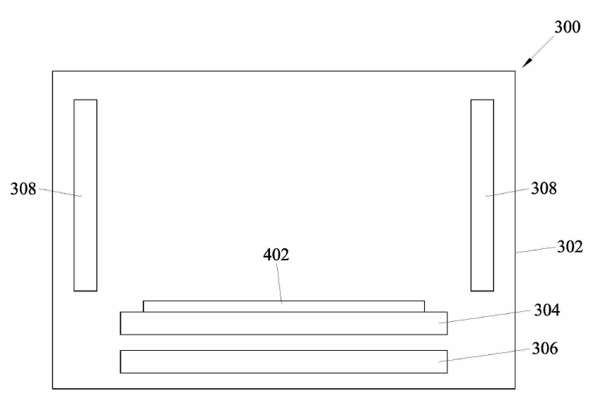
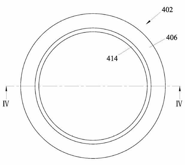
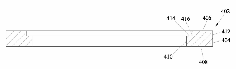
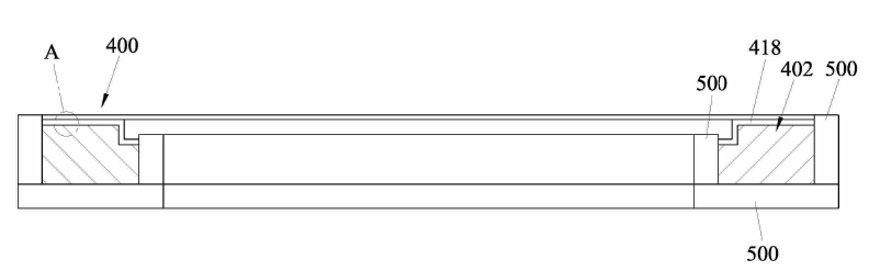
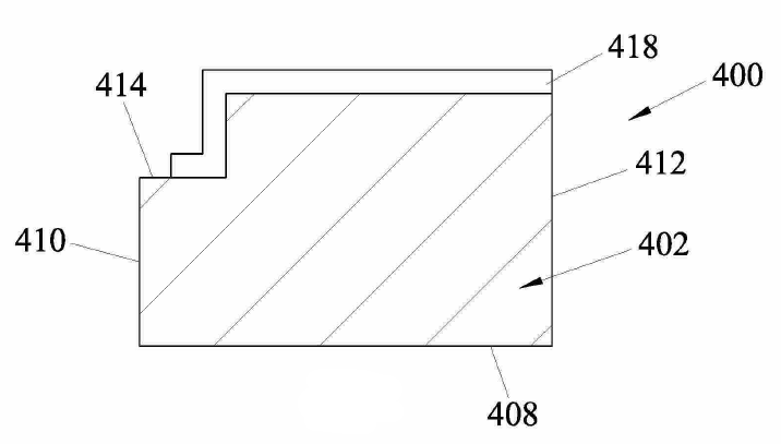
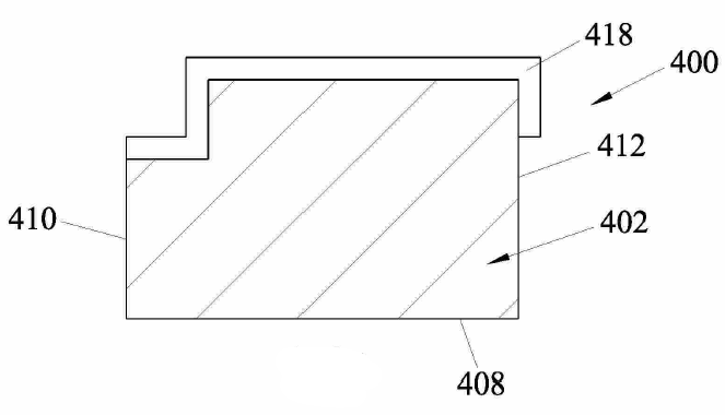
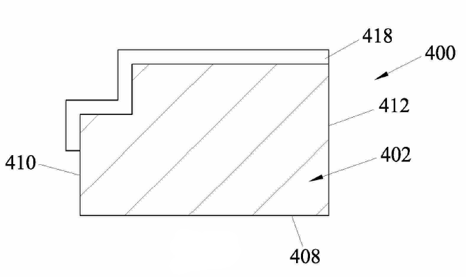
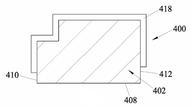
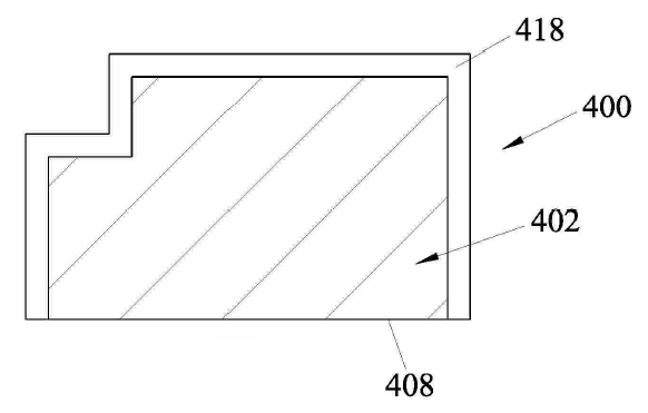
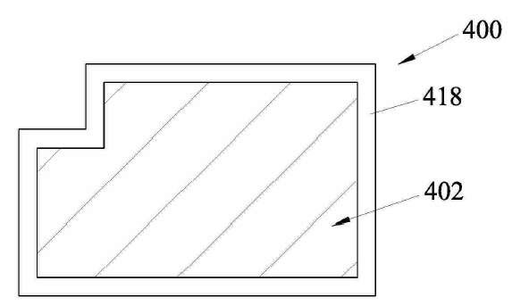
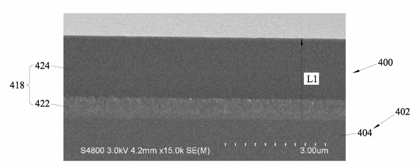
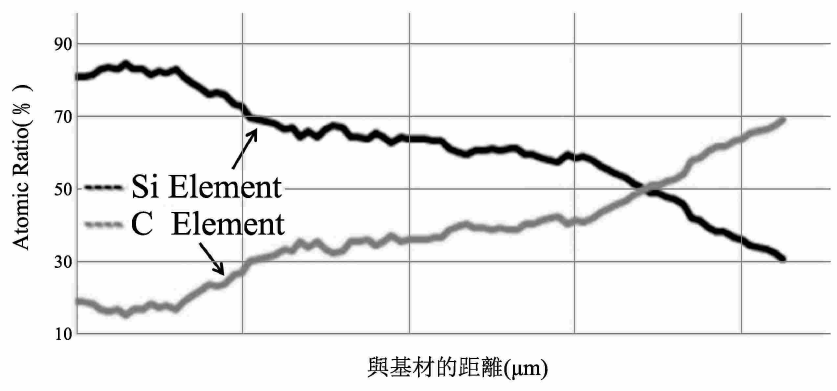
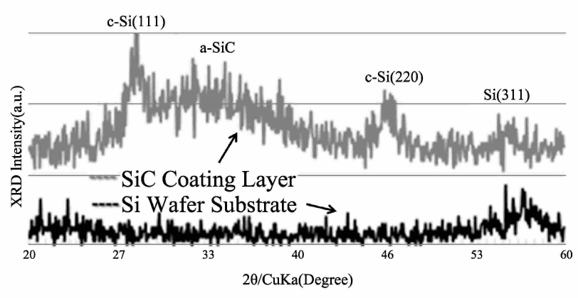
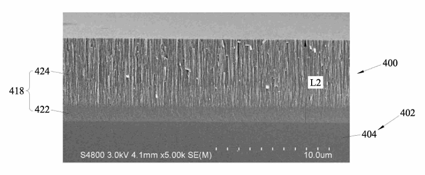
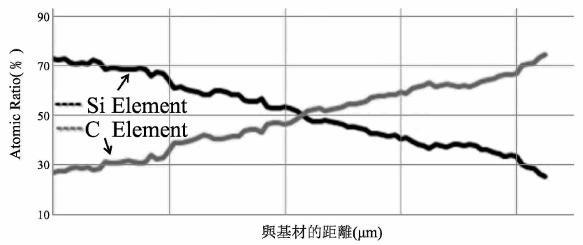
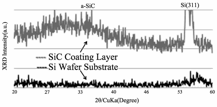
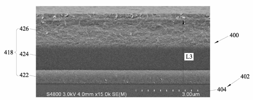
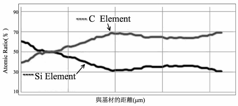
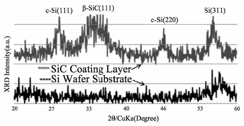
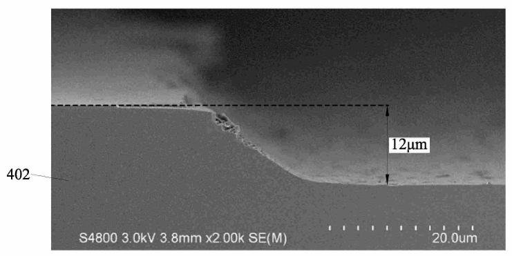
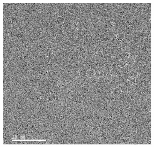
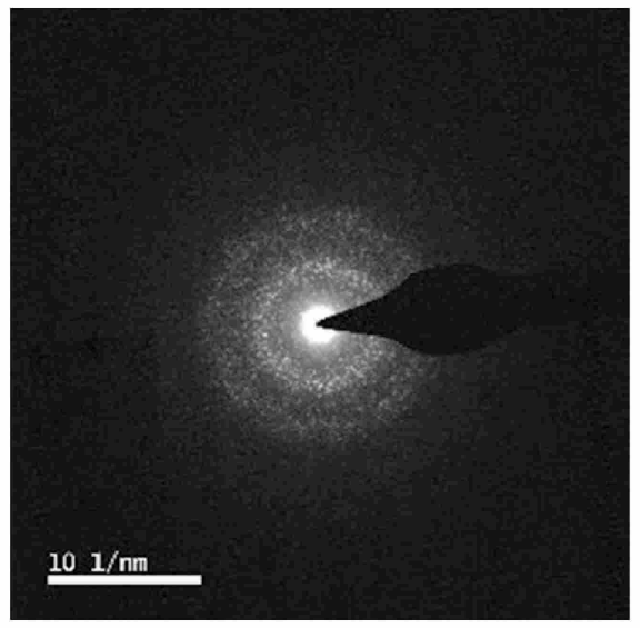
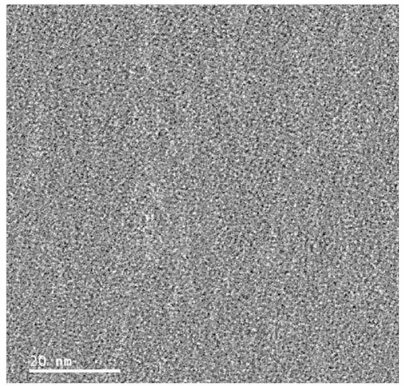
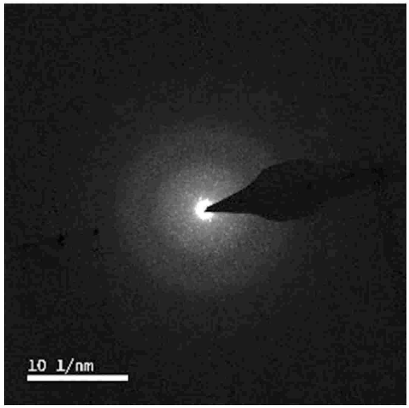
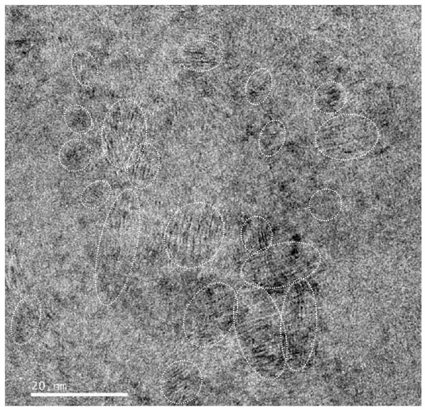
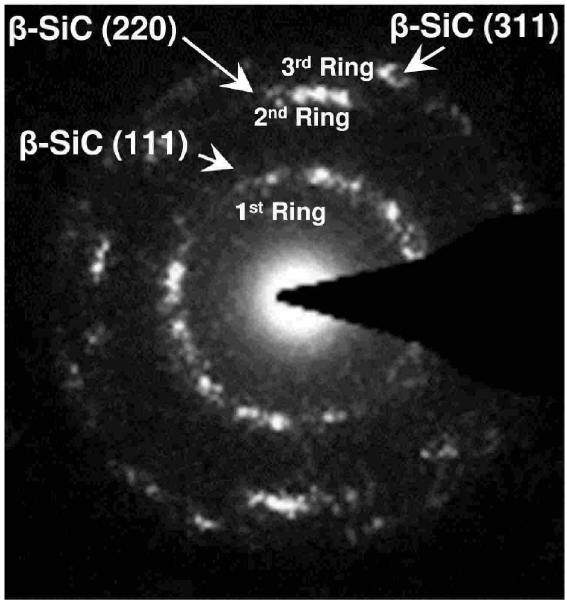
Other features and effects of the present invention will be clearly presented in the embodiments with reference to the drawings, wherein: Figure 1 is a flowchart illustrating some embodiments of the manufacturing method of the component of the present invention, the component being suitable for use in semiconductor process equipment; Figure 2 is a schematic diagram illustrating a reactive physical vapor deposition equipment for performing the method according to some embodiments of the present invention; Figure 3 is a top view schematic diagram illustrating a substrate of the component according to some embodiments of the present invention; Figure 4 is a cross-sectional view taken along line IV-IV of Figure 3; Figure 5 is a schematic diagram showing a protective coating formed on the substrate; Figures 6 to 11 are schematic diagrams illustrating different variations of the protective coating; Figures 12 and 13 show different arrangements of silicon targets in the reactive physical vapor deposition equipment; Figure 14 is an enlarged schematic diagram showing a plurality of microstructures of the substrate; Figure 15 is an enlarged schematic diagram showing a variant where the microstructures of the substrate have a pyramid shape; Figure 16 is a scanning electron microscope (SEM) image of a specific example of the component; Figure 17 shows energy-dispersive X-ray spectroscopy (EDS) analysis results of the protective coating of the specific example shown in Figure 16; Figure 18 shows X-ray diffraction (XRD) analysis results of the protective coating of the specific example shown in Figure 16; Figure 19 is an SEM image of another specific example of the component; Figure 20 shows EDS analysis results of the protective coating of another specific example shown in Figure 19; Figure 21 shows XRD analysis results of the protective coating of another specific example shown in Figure 19; Figure 22 is an SEM image of yet another specific example of the component; Figure 23 shows EDS analysis results of the protective coating of yet another specific example shown in Figure 22; Figure 24 shows XRD analysis results of the protective coating of yet another specific example shown in Figure 22; Figures 25 to 28 are SEM images illustrating microscopic images of the substrate and microscopic images shown in Figures 16, 19, and 22 after being etched by reactive ion etching (RIE) process; and Figures 29 to 34 show high resolution transmission electron microscope (HRTEM) images and diffraction patterns of samples shown in Figures 16, 19, and 22.
【Figure 1】
【Figure 2】
【Figure 3】
【Figure 4】
【Figure 5】
【Figure 6】
【Figure 7】
【Figure 8】
【Figure 9】
【Figure 10】
【Figure 11】
【Figure 12】
【Figure 13】
【Figure 14】
【Figure 15】
【Figure 16】
【Figure 17】
【Figure 18】
【Figure 19】
【Figure 20】
【Figure 21】
【Figure 22】
【Figure 23】
【Figure 24】
【Figure 25】
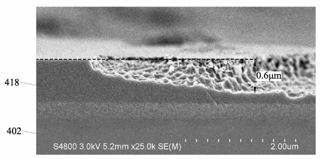
【Figure 26】
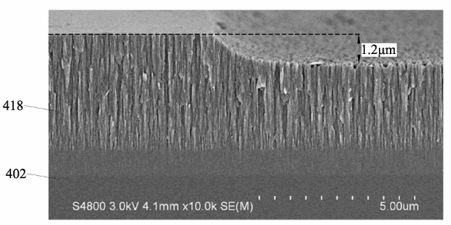
【Figure 27】
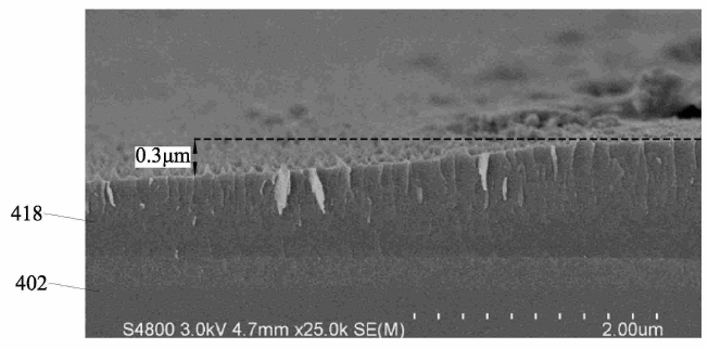
【Figure 28】
【Figure 29】
【Figure 30】
【Figure 31】
【Figure 32】
【Figure 33】
【Figure 34】