Optical Multilayer Film and Its Applications
Patent Certificate Number: I766688
Title: Optical Multilayer Film and Its Applications
[1] Scope of Patent Application
- An optical multilayer film, comprising: a substrate; a first coupling layer disposed on the substrate, including at least one first dielectric material layer and at least one second dielectric material layer stacked alternately to form a multilayer structure, wherein the first dielectric material layer comprises titanium dioxide, tantalum pentoxide, niobium pentoxide, aluminum nitride, or aluminum oxynitride, and the second dielectric material layer comprises magnesium fluoride, silicon dioxide, or alumina; a conductive layer disposed on the first coupling layer; and a second coupling layer disposed on the conductive layer, wherein the first coupling layer is located between the substrate and the conductive layer.
- The optical multilayer film according to claim 1, wherein the substrate has a first surface and a second surface opposite to the first surface, and the optical multilayer film further comprises an anti-reflective coating disposed on the first surface of the substrate, wherein the first coupling layer, the conductive layer, and the second coupling layer are disposed on the second surface of the substrate.
- The optical multilayer film according to claim 1, wherein the sheet resistance of the conductive layer ranges from 10 Ω/□ to 250 Ω/□.
- The optical multilayer film according to claim 1, wherein the sheet resistance of the conductive layer ranges from 10 Ω/□ to 30 Ω/□.
- The optical multilayer film according to claim 1, wherein the thickness of the conductive layer is greater than 50 nanometers and less than or equal to 400 nanometers.
- The optical multilayer film according to claim 1, wherein the reflectance of the optical multilayer film at wavelengths from 400 nanometers to 700 nanometers is between 0.1% and 5%.
- The optical multilayer film according to claim 1, wherein the reflectance of the optical multilayer film at wavelengths from 400 nanometers to 700 nanometers is between 0.1% and 1%.
- The optical multilayer film according to claim 1, wherein the substrate is non-planar in shape.
- The optical multilayer film according to claim 8, wherein the substrate has a first surface and a second surface opposite to the first surface, the first surface of the substrate is convex, and the second surface is concave.
- The optical multilayer film according to claim 1, wherein the conductive layer is made of a transparent conductive material.
-
Use of the optical multilayer film according to claim 1, applied for anti-reflection, heating defogging, and heating defrosting.
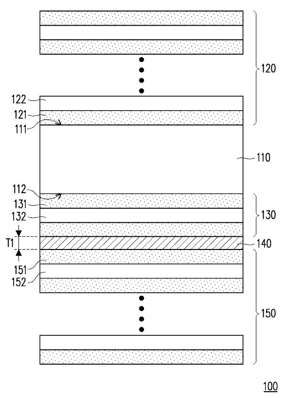
- Figure 1 illustrates a cross-sectional schematic diagram of the optical multilayer film according to the first embodiment of the present invention.
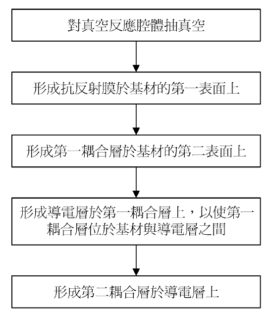
- Figure 2 is a flowchart of the manufacturing method for the optical multilayer film according to the first embodiment of the present invention.
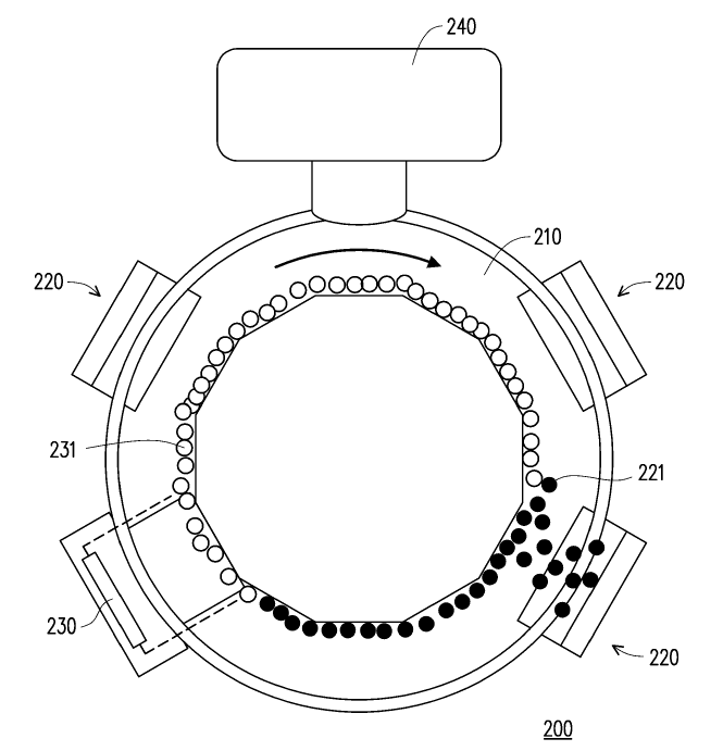
- Figure 3 shows a top view schematic diagram of the vacuum coating equipment.
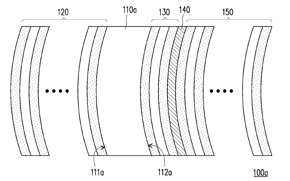
- Figure 4 illustrates a cross-sectional schematic diagram of the optical multilayer film according to the second embodiment of the present invention.
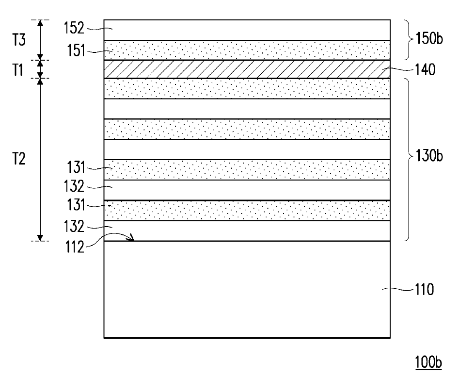
- Figure 5A illustrates a cross-sectional schematic diagram of the optical multilayer film according to the third embodiment of the present invention.
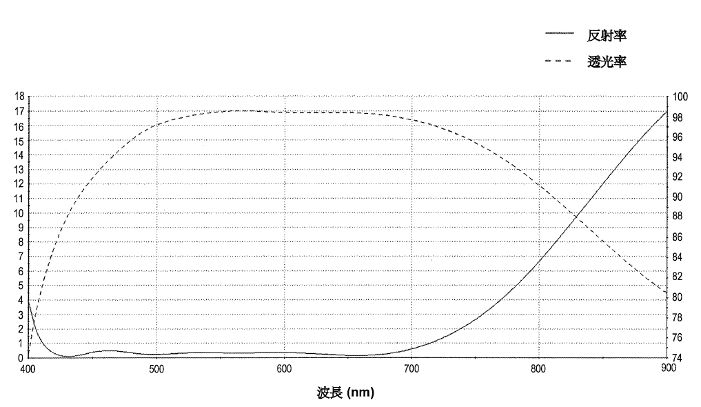
- Figure 5B shows the reflectance and transmittance of the optical multilayer film of the third embodiment shown in Figure 5A at different wavelengths.
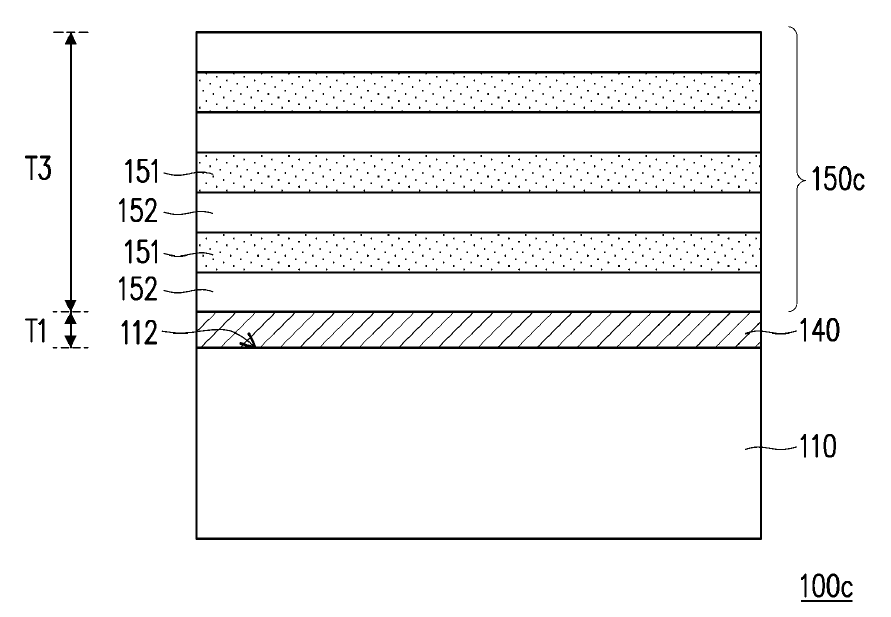
- Figure 6A illustrates a cross-sectional schematic diagram of the comparative example of the optical multilayer film.
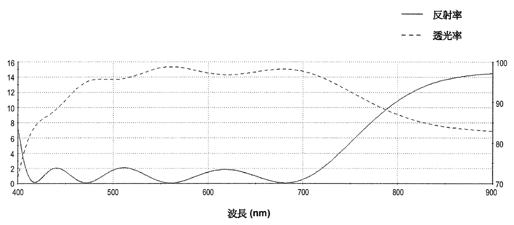
- Figure 6B shows the reflectance and transmittance of the comparative example shown in Figure 6A at different wavelengths.
【Figure 1】
【Figure 2】
【Figure 3】
【Figure 4】
【Figure 5A】
【Figure 5B】
【Figure 6A】
【Figure 6B】