Activated Reactive Magnetron Sputtering
Process principle of activated-reactive-magnetron-sputtering
The progress of coating technology has led to the development of industries such as optoelectronics, machinery and semiconductors. Many novel film properties such as optical, electrical, magnetic, energy and mechanical properties have been developed one after another. Nowadays, DC magnets are often used in coating processes in the display, touch panel and semiconductor industries. Controlled sputtering technology, through the improvement of power supplies and different reactive gases flow to form compound films of different compositions , also known as reactive sputtering, the theoretical basis of reactive sputtering is based on the hysteresis phenomenon, but there are three main problems with reactive sputtering:
- Hysteresis effect.
- Poisoning of the target surface causes arcing.
- Disappearing anode effect.

Figure 1. (a) Nitrogen partial pressure-nitrogen flow hysteresis curve, (b) oxygen partial pressure-oxygen flow hysteresis curve
Figure 1 (a) and (b) are the schematic diagrams of the hysteresis curves of nitrogen partial pressure-nitrogen flow and oxygen partial pressure-oxygen flow, respectively. It shows that as the flow of reactive gas increases, the surface of the target material changes from the metal state to the transition state. Poisoned state, the surface of the metal target is gradually covered by dielectric to form an insulating layer. This insulating layer can be regarded as a parallel electrode plate, which causes argon ions to accumulate charge. When the positive charge accumulates too much, it will break down with the target. Phenomenon (this phenomenon is called arcing), accompanied by high temperature and high heat, evaporates larger particles, which reduces the film quality and affects the optical properties. As shown in Figure 2, it is to eliminate arcing and plasma caused by the hysteresis in the reactive sputtering process. Density instability leads to problems such as film quality and process instability. The concept of a Activated Reactive Magnetron Sputtering process appears [8]. The process system has a target area and a plasma source area. This plasma source area can also be called a coupled electroplating process. Pulp area. During the process, an inert gas is introduced into the target area, and a mixed reactive gas is introduced into the plasma area, so that the target is not affected by the reactive gas during the sputtering process. The process has high stability and still maintains the sputtering process. Advantages of high film quality, large area and high uniformity.

Figure 2. Schematic diagram of film defects caused by Arcing

Figure 3. Schematic diagram of different reactive gas fluxes forming dielectric on the target surface
As shown in Figure 3(a), when reactive sputtering is in a low reactive gas flux, the target is in a metallic state, and reactive gases are not easy to form compounds on the surface of the target. Almost all reactive gases are used to form compounds; As the flow rate of the reactive gas increases, compounds are gradually formed on the surface of the target, as shown in Figure 3(b)~(d) above [9], which in turn affects the process stability and deposition rate. In order to avoid the influence of reactive gases on the process, the sputtering and reaction are divided into two stages [10]: the cathode target sputters the target particles, which are attached to the substrate surface to form an ultra-thin metal film with a thickness of about 1 to 4 Å, and Generate reactive gas plasma in a closed area to make reactive gases such as oxygen and nitrogen gas radicals react with the ultra-thin metal on the surface of the substrate, and form a variety of reactants, such as SiOx, NbxOy or SixNy compounds through the mixed gas ratio, This is the nucleation stage of film growth. Repeat the above process to make the target particles continuously react and condense to form a dielectric film. The interaction between sputtering and reactive gas is separated to eliminate charge accumulation, arcing and manufacturing process. It is unstable and achieves the effect of high deposition rate. This process method is called Activated Reactive Magnetron Sputtering method [11], as shown in Figure 4.
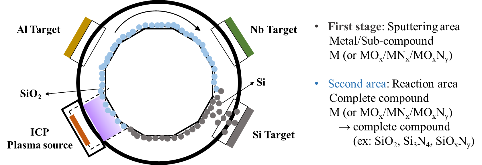
Figure 4. The intention of the Activated Reactive Magnetron Sputtering process
Process advantage of Activated Reactive Magnetron Sputtering
By separating the interaction between sputtering and reactive gas, the shortcomings of the reactive sputtering process can be effectively improved. In addition to the advantages of high film quality and large-area uniformity of the sputtering process, the process has higher stability and It is comparable to the high deposition rate of the sputtering target metal.

[1] J. Čapek and S. Kadlec, "Return of target material ions leads to a reduced hysteresis in reactive high power impulse magnetron sputtering: Experiment," Journal of Applied Physics 121, 171911 (2017).
[2] S. Berg, H. ‐O. Blom, M. Moradi, C. Nender, and T. Larsson, "Process modeling of reactive sputtering," Journal of Vacuum Science & Technology A: Vacuum, Surfaces, and Films 7, 1225–1229 (1989).
[3] A. H. Simon, "Sputter Processing," in Handbook of Thin Film Deposition (Elsevier, 2012), pp. 55–88.
[4] K. Koski, J. Hölsä, and P. Juliet, "Deposition of aluminium oxide thin films by reactive magnetron sputtering," Surface and Coatings Technology 116–119, 716–720 (1999).
[5] H. Kakati and S. M. Borah, "Study of hysteresis behavior in reactive sputtering of cylindrical magnetron plasma," Chinese Physics B 24, 125201 (2015).[6] Y. H. Han, S. J. Jung, and J. J. Lee, "Deposition of TiO2 Films by reactive Inductively Coupled Plasma assisted DC magnetron sputtering for high crystallinity and high deposition rate," Surface and Coatings Technology 201, 5387–5391 (2007).
[7] C. A. Bishop, "Reactive Sputter Deposition," in Vacuum Deposition onto Webs, Films and Foils (Elsevier, 2011), pp. 375–387.
[8] shingo samori, T. Sugawara, S. Agatsuma, M. Ishida, S. Yamamoto, M. Miyauchi, Y. Jiang, and E. Nagae, "RAS Bias Voltage Coating," in Optical Interference Coatings (OSA, 2013), p. WC.3.
[9] R. Chodun, K. Nowakowska-Langier, and K. Zdunek, "Methods of optimization of reactive sputtering conditions of Al target during AlN films deposition," Materials Science-Poland 33, 894–901 (2015).
[10] F. Huang, B. Xie, B. Wu, L. Shao, M. Li, H. Wang, Y. Jiang, and Y. Song, "Enhancing the crystallinity and surface roughness of sputtered TiO2 thin film by ZnO underlayer," Applied Surface Science 255, 6781–6785 (2009).
[11] D. Noguchi, T. Eto, K. Kodama, Y. Higashimaru, S. Fukudome, Y. Kawano, F. Sei, and I. Siono, "Technique for High-Rate, Low-Temperature Deposition of TiO 2 Photocatalytic Thin Film Using Radical-Assisted Sputtering," Japanese Journal of Applied Physics 50, 010204 (2011).